Printed Circuit Board Design Basics for machines
First and foremost acknowledge that creating a perfectly optimised printed circuit board for production can be very simple or very complicated. If you are in control of all the processes this will help. If you are not, then think of your goal as being an active member of a team working for the best results possible. Note that printers, assembly machines, electronic and optical testers, like ourselves, are not created equal. These pages are written to help you achieve a good design, minimising the difficulties for the subsequent phases of assembly and testing of your PCB. I also share some of the common knowledge that new operators/programmers of the various machines involved in this process should be aware of.
Fiducials
You may be wondering, "Why has Kevin opened the discussion of Printed Circuit Boards (Pcbs) here with fiducials?". Fiducials are the start of many processes for many machines. Not understanding fiducials is one of the best ways to shoot yourself in the foot. Yes, I have seen many programs reduced to trash because of fiducials and inadequate knowledge thereof. If you are a programmer that is unsure or not yet schooled on the ramifications of changing fiducials then please take the following words of advice.
Do not alter Fiducials!
I have said this to dozens of programmers and still often they insert lead into their feet (shooting themselves). Okay, with some direction, experimentation and patience you can learn how to work with fiducials but this is an advanced topic, not always working the same for different software so beware and be careful, go "Leadfree".
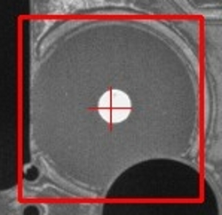 Fiducial Mark - RefDot10
- Once a printed circuit board (PCB) has been transported or placed into a machine the board's exact position must be calculated. Dependent on the particular machine this may be done with locating holes but most often done with Fiducials. The machine's cameras are programmed to search a specific area and match a specific pattern of bright and darker pixels, a fiducial. With it's found image the software will calculate a center point position. With the center point position of two or more fiducials software can determine the position and stretch/shrinkage of the PCB.
- A fiducial mark is most often created at the same time as the pads that will be used to solder the components on the PCB. The producer of the PCB must know the form and position of the fiducial. It is important to realize as a person involved in the process of creating a PCB for machines the significance of information about fiducial positions in respect to component positions. Layout software for PCBs can produce CAD data formats containing the center point information for fiducials and components. Supplying the production, assembly and testing machines with design stage center point data is your best method to get the best results in the shortest time from the complete process.
- Gerber data often used by producers of PCBs is not a convenient format. This data will include information about all the layers, traces, pads and etc. needed to produce the PCB. Center point data is often not included and difficult to decode. Many other CAD formats are available.
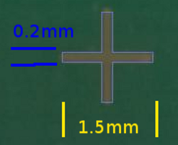 A Better Fiducial Mark
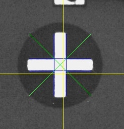
- The designer of the fiducial mark (reference mark) above has done a good job in a couple of respects. There is enough free space around the fiducial for a good match and the protective finish for the board has not been applied on this area making a good contrast possible. The form of a circle is considered by some individuals to be an industry standard. As a programmer and operator of various machines I find the form of a cross to be much more accurate and well supported. My optimal fiducial is shown on the left.
- This mark is only 50% larger than a 1mm dot and allows software designers a much better chance for higher accuracy. The Zentroid name for this mark is RefCross15x02.
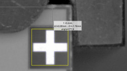 Please do not jam in Corners!
- Many designers flow the rule, "Place reference marks as far as possible from each other for better accuracy". Although there is some truth to this rule there are several other considerations. In this case this Orprovision machine can luckily evaluate the fiducial because the transport's rail stops short of the stopper. A fiducial in the upper left of this PCB would be useless.
- A good rule of thumb is to keep the outermost part of all fiducials at least 5mm from the finished edge of any PCB or panel thereof.
- The Zentroid name of this fiducial is RefCross25x06.
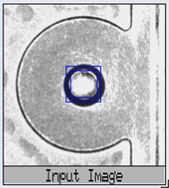 Ensure a good contrast with a suitable margin.
- This image is taken from Viscom's excellent debugger level. There are a couple of things to notice from this image.
- First and foremost is that the designer of this printed circuit board has provided lots of room for the fiducial mark but the dark contrast area is much too small. The bright area outside of the fiducial will effect the position calculation of the fiducial itself. Notice that the fiducial is not exactly centered within the dark area.
- Another point of interest is the mark itself. As is often the case, the surface of the mark has been tinned. This can make the surface of the mark irregular. In this case you can see the shadded areas. This effect can be very significant for the dot shape. I have seen many examples were the calculated middle position of the mark can have a tolerance as large as 25% of the width of the mark itself. For this reason I prefer the shape of a single cross for fiducial marks.
 Here starts the fun and games!
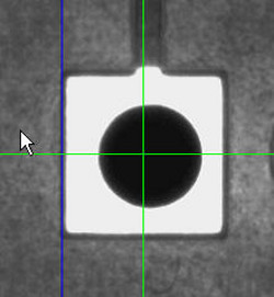
- This is an image of Zentroid's RefRect20. A PCB without fiducial marks is simply poorly designed! Without fiducials machine programmers start having to be creative. Let's look at this example. The machine's software will likely provide you with a way to add fiducials to the PCB but what do you choose. Look closely at the image on the left.
- If you and your software are up to the challenge use the outside form of pads if you have to use pads. My 2mm rectanglar/square reference mark (fiducial) has been accurately located. The hole in this pad is not centered. It is common for drill data, data used by the machines to drill the holes, to have a significantly large tolerance. Having the most accurate data possible will help greatly when it comes time to test your PCBs in any AOI System.
 Consider the possibilities!
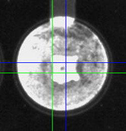
- Often forgotten when dealing with THT applications is the fact that AOI machines can effectively test wave soldered assemblies. In this case providing a fiducial protected from the soldering process would be a great advantage to AOI programming. As seen in this image the average brightness of the tht solder joint is centered to the left. The software has indicated with the green cross the evaluated middle of this image. Finding a suitable image to use as a replacement for a fiducial can in some cases be very frustrating. By the way the Zentroid name for this pseudo fiducial is RefThtDot22
 With fiducials like this your team/machines will have a great start!
- I hope this basic introduction to fiducials will help you to make your process of creating, assembling and testing of PCBs as efficient and problem free as possible. I know as an instructor and programmer of various machines included in this process that careful preparation of fiducials and their data will be a worthwhile effort. You may also some day put a smile on my face or on the face of one of the many other person's involved in programming our machines!
