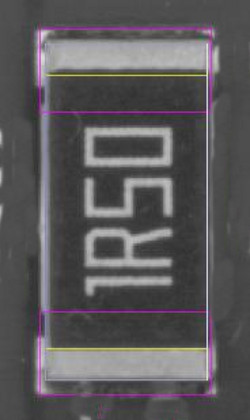
 This resistor's pads are too small!
- Small pad size can render your AOI testing useless. Most testing of chip components is done from orthogonally mounted cameras. Top view FOVs generally meet the needs of chip testing and are faster than including angled FOVs (Field Of View)s. To be tested this component to our left would demand angled views due to the very small pad area left for the solder joint fillet. Without angled testing, should one end of this resistor be slightly lifted most AOIs will not indicate a fault.
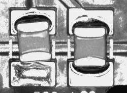 Pads must contact the complete Pin mating surface!
- The foremost problem here is the separation of the pads and secondly they are just a little large. As solder melts surface tension forces will try to pull both pin's contact area towards the middle of the pads. It is a little like a tug-of-war. Often the forces become unbalanced enough that the component, our cc3025x16, will be pulled onto one pad leaving the other as a lifted lead. Most manufactures of SMD devices include their recommended pad geometry in their data sheets and I recommend that when designing PCBs you should be aware of these recommendations and not deviate greatly from them.
AOIs need Fillets!
Not fresh or salt-water but solder fillets. These are the places (cracks or corners) on your assembled PCBs where molten solder will flow into. If the solder can flow into a joint making a fillet then some of the pad edges may have very little remaining solder there. Often an AOI can be programmed to evaluate the amount of solder at the joint and pad edges. If in your line or process you have checked for applied solder paste then even a top camera only AOI system can provide reliable testing results. Above when commenting about the capacitor and it's pad layout I suggested that the manufacturers recommendation should be considered. For more involved packages you may not find such information so let's look at an example...
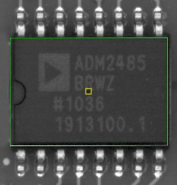 udg16_127p103x25 layout
- If I were to create an equation for the amount of space to provide between an ICs pin and the pad outer edge I would have to consider the following criterion.
-
- Length of the pins mating surface to the pad.
- Exit angle of the pin from the pad.
- Solder volume applied to the pad.
- Area of the pad.
- Area of the pin on the pad.
- Thickness of the pin.
- Position tolerance of the pin.
- Form of the pad end.
- From this list you can see that an analytical solution would be very complicated and involve factors you may not know. We will proceed in with a general discussion that you should be able to apply. The standard component shown is barely if at all suitable for attaining "No False Call" testing. Notice that the component is perfectly centered. Your position tolerance in the direction of the width of this component will likely put the component completely off the pads, therefore the pads must be lengthened.
- Solder moving away from the pad edges is from the capillary action of the melted solder. Even with this IC positioned perfectly there is very little space to evaluate this effect. The rounded pad ends are also not ideal for capillary testing, rectangular pad ends are much better.
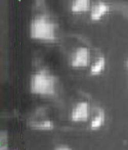 Pin Solder Joint
- This angled view of the pins of the above IC are taken with a current Orprovision AOI. The distance of the pin to pad outer edge is 0.33mm. From the heal to the inner edge is 0.7mm. You can see that a large amount of the solder will flow to the heal side of the pin. A fillet also forms at the pin end leaving very little room for capillary testing of the pad. In some processing environments the pin end fillet is not well formed (often due to poorly prepared component pin ends) making capillary testing a very interesting option, one that needs some space.
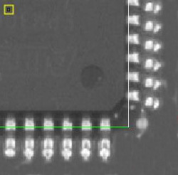 uqg44_80p120x11
- These pins have a distance of 0.3mm to the pad outer edge. My opinion of the pad layout is the same as for the pins shown above. In this case however the tolerance I would allow is significantly less and therefore I would not have to extend the pad length as much as in the example above.
- I have been asked to name a simple "Ball Park" figure (measurement) for pin end to pad outer edge. You can use my rules of thumb at your own risk! I am also aware that many other factors can come into play like high-density layouts. You must evaluate the advantages and disadvantages and then live with them.
-
- Dual pin group packages -> 5 to 6 times the pin height (minimum).
- Quad pin group packages -> 2 to 3 times the pin height (minimum).
 This resistor's pads are too small!
 Pads must contact the complete Pin mating surface!
 udg16_127p103x25 layout
 Pin Solder Joint
 uqg44_80p120x11